Содержание
Готовые модули
Обзор готовых плат
Небольшой обзор на tpa3116 d2 можно посмотреть в видеоролике. В нём протестированы возможности по максимальной мощности и частотные характеристики. Чтобы начать прослушивать музыку достаточно подключить плату к блоку питания, источник звука и внешние динамики. Найти в продаже модуль стереоусилителя 2×50вт на tpa3116d2 не составит особого труда. Цена таких плат начинается с 700 рублей, в зависимости от назначения и дополнительного функционала. Перед применением желательно проверить наличие термопласты между радиатором и усилителем.
Модуль в авто
Для применения tpa3116d2 в автомобиле потребуется доработка. Так как бортовой сеть машины рассчитана на 12-14 В, то максимальная выходная мощность усиления не превысит 15-20 Вт и вряд ли устроит автолюбителя. При попытке повысить это значение путём увеличения громкости — появляются шумы и искажения, что естественно не приемлемо для прослушивания музыки. Для решение данной проблемы как минимум потребуется дополнительный преобразователь напряжения с 12 до 24 В, который иногда в разы дороже самой микросхемы. Вариант усилителя с уже установленным на плате повышающим инвертором представлен в следующем видеоролике.
https://youtube.com/watch?v=awFu6QRbeug
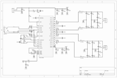
Step 6: Power Amplifier
As they say, save the best for last!
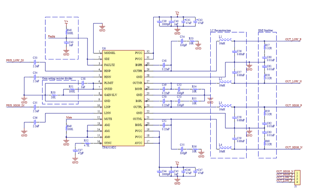
The most important circuit of all, the TPA3118 power amplifier circuit, ripped shamelessly straight from the TI application notes.
FAULTz is an open drain output pin that is driven low if the chip encounters any type of fault, including over temperature, over current, and DC offsets at the input. This is directly connected to SDz, a pin that shuts down the chip. The appended «z» indicates that these signals are active low. This means that the chip will be shut down every time a fault is indicated, a good safety measure.
It is very important to note that the TPA3118 has internally biased differential inputs — meaning, if you connect any of the inputs straight to ground the TPA3118 will NOT like it (it will drive the FAULTz pin low). Each positive and negative input should be AC coupled. Even if the negative inputs are simply referenced to ground (i.e. single ended), they should still be connected through a capacitor. These 2.2uF coupling capacitors are film capacitors to prevent distortion.
R50 and R52 set the gain of the TPA3118. Here it is set to 26dB. Consult page 14 of the TPA3118 datasheet for other options.
The MUTE control can be used to prevent startup pop. I have not implemented this in this board. To mute the TPA3118, hold this pin to a logic high (above 2V).
Each side of the TPA3118 has a series of bulk and decoupling capacitors (C39-43, C44-C7). The two 47uF electrolytics can easily be replaced with one 100uF. I had a lot of space on the board but not much vertical room, so two shorter capacitors were better than one taller capacitor. Here is a very comprehensive application note about LC filters in Class-D amplification.
The output connector, is a screw terminal block.
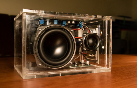
Step 8: Speaker Box
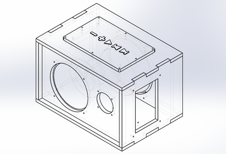
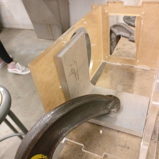
I designed a simple dovetail jointed box intended to be laser cut from acrylic. The .step file and .dxf files I used for laser cutting are attached here. The internal volume is about 2L without any components, so effectively it will be approximately 1.5L with everything in (the same as the modeled volume from before). The holes are actually only used for drill guides, and should be drilled bigger depending on the screw used. The top panel was originally going to be a conductive 3D printed capacitive touch panel printed on the Voxel8 Developer’s Kit. However, I never ended up designing the microcontroller that was to use this panel. The side panel was purchased from DigiKey and is reflected in the BOM.
Note that laser cut acrylic has a bevel on the edge, meaning it is not entirely flat. I was concerned about using acrylic cement with this beveled edge, and so I used epoxy, which is not ideal for acrylic as it does not bond quite well. However, the box seems sturdy thus far although no drop tests have been done 😀
A very handy piece of right angled aluminum I found was used in the gluing process to keep things square.
Step 1: Component Selection
Here are some descriptions about the ICs and components I used.
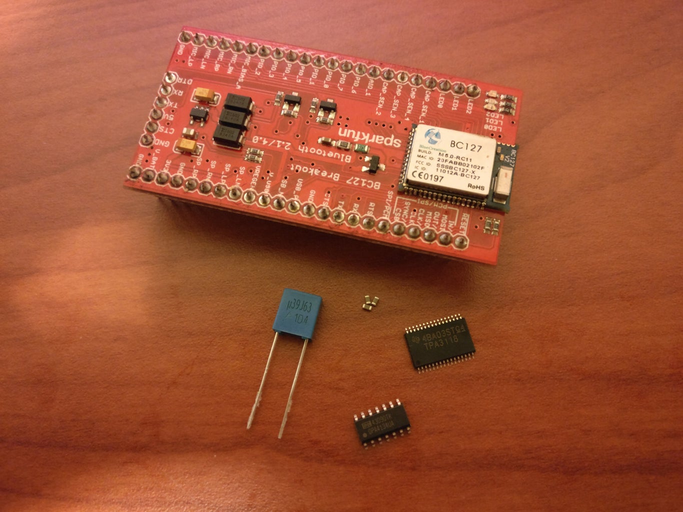
TPA3118
This is the single most important chip on this PCB — after all, it literally is the amplifier.
The TPA311x is a family of Class-D amplifier chips made by Texas Instruments (TI). Class-D is an extremely efficient method of amplification, with upwards of 90% power efficiency, greater than the more traditional Class-A (50% theoretical maximum efficiency), Class-AB/B (78.5% theoretical maximum efficiency). This means that Class-D will generate less heat, and a battery would last longer, making it perfect for portability.
Texas Instruments offers very clear and helpful datasheets and very responsive technical support, making designing with this chip easier for a beginner designer.
BC127
The BlueCreations BC127 is a very comprehensive Bluetooth audio module with a built in antenna, making Bluetooth integration into PCB projects quite easy. It has a fairly low current draw of 16mA while streaming music, support for playback control (next, previous, volume, play/pause) and a UART based firmware programming system.
OPAx134 Operational Amplifier
The OPAx134 family was selected for the preamplifier and filter sections because it is a frequently used op amp. It is made, again, by TI (they bought Burr-Brown) and is a very high quality audio-optimized op amp. However, it is not necessarily the best op amp for this particular application (will be explained in more detail later).
Voltage Regulators
There are two linear voltage regulators on this board. A 3.3V regulator provides power to the BC127. A second adjustable linear voltage regulator provides a constant reference voltage for the op amps.
Capacitors
While capacitors are simple passive components, and there may be a large amount on any given PCB, their selection process is quite complex. Capacitors are made of many different types of materials, each with its own characteristics. Different types of capacitors are used for different purposes and may not be interchangeable.
The cheapest and most common type of capacitor is the ceramic capacitor. These would be a no-brainer because of the price and size, except for a major caveat — their capacitance changes based on the voltage across the capacitor. At lower voltages this change is not particularly significant, however audio tends to have fairly high voltages (enough to make ceramic capacitors vary significantly in capacitance). This causes significant harmonic distortion in the signal and degrades audio quality significantly.
The film capacitor is recommended for use in audio. They have much more constant characteristics. However, not every capacitor in the circuit has to be film — film capacitors are many times more expensive than ceramic capacitors and this would make our circuit extremely costly!
Therefore, I used a mix of ceramic and film capacitors in the audio path. Smaller values of ceramic capacitors (up to nF) are available in an C0G/NP0 rating, meaning they have no voltage or temperature coefficient and they can be used directly in the signal path. However, for larger coupling and filter capacitors, film capacitors should be used.
Connectors
My connector of choice is the JST PH series. They are very commonly available 2.0mm pitch connectors, with a smaller footprint and cheaper than 2.54mm connectors like the Moxel C-Grid. I use these to connect all of my off board connections (switches, potentiometers, etc.).
Основные характеристики
Согласно datasheet, tpa3116d2 рассчитан на работу с внешними динамическими головками на 100 Вт с нагрузкой 2 Ом в монорежиме. Также способна обеспечить выходную мощность на два канала (2×50 Вт) на 4 Ом – мостовая схема. Стоит учитывать, что данные значения можно получить только при подаче на плату напряжения от блока питания на 24 В с током на 6 А. На двух микросхемах можно собрать современный стерео усилитель на 100 Вт класса D. При этом на каждый канал будет использоваться по одному устройству. Такие изделия сильно греются при работе, поэтому для них в обязательном порядке применяется радиатор.
Максимальные параметры
Рассматриваемое устройство характеризуется низким уровнем нелинейных искажений (<0,1%) и высоким значением отношения сигнал/шум (102 дБ) на выходе. Оснащено встроенной защитой от короткого замыкания, перегрева, превышения предельного значения постоянного тока, повышенного и пониженного напряжения.
Предельные значения основных эксплуатационных характеристик tpa3116d2:
- выходная мощность (PO):
- 2×50 Вт (стерео); 1×100 Вт (моно);
- максимальное питание (VCC) до +30 В;
- напряжение на аудиовходах (VI) от -0.3 до 6.3 В;
- коэффициент нелинейных искажений (THD) < 0.1%;
- частота ШИМ — до 1,2 МГц;
- температура: рабочая (ТА) от -40 до +85 oC; кристалла (ТJ) от -40 до +150 oC; хранения (Тstg) от -40 до+120 oC.
Несмотря на то, что рассматриваемое изделие имеет механизмы защиты не рекомендуется превышать указанные параметры.
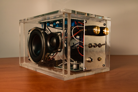
Step 9: Final Assembly and Notes
After receiving your PCB (mine are from PCBWay), the fun times of populating the board begins! If you have access to a reflow oven, get a stencil made and use the reflow oven! This would have saved a few hours of hand soldering and makes solder bridges less likely. Although the components on my layout are small, they can all be done by hand (I’ve done it twice). Be sure to check for shorts on your PCB (the tight footprints anyways) with a multimeter before turning it on. The BC127 especially has quite a fragile output section that can easily break.
The front and back panels are inset so that the speakers have room to vibrate in case a grille is installed.
The amplifier can be powered using any 9-12V power supply, including wall warts and batteries. A battery pack of 3 lithium-ion batteries with a charging module(I believe http://www.batteryspace.com/ has some) would be the ideal power source because it offers a nominal voltage very close to 12V.
I did not include any designs of my power supply as I am currently using a PCB I have designed that doesn’t quite work right (will keep trying).
After powering the speaker up after many days of debugging, I noticed a few things:
— the midrange is very clean
— the speaker is very loud and has a pretty serious bass capability for its size
— the speaker works better without the Linkwitz Transform because of op amp clipping
— the entire amplifier draws about 200mA at a low volume, and potentially 500mA to 1A at full volume — note this for battery and power supply choice
An unfortunate soldering accident with my BC127 module left me without Bluetooth on this speaker. Once I get more of them (on sale at Sparkfun right now!) I will replace it.
Woo!
Step 2: Speaker Drivers and Simulations
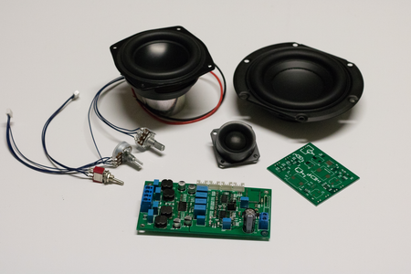
While the amplifier is the focus of this Instructable, inevitably the driver choice affects some component values in the amplifier. Here’s a quick description of the speaker drivers that I am using.
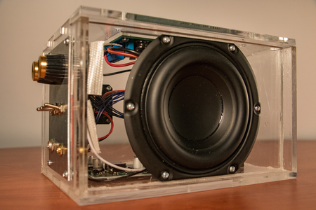
Dayton Audio ND91-8
The Dayton Audio ND91-8 is a small, 3.5 inch driver capable of some impressive bass for its size (who doesn’t love bass?). Realistically, a higher impedance driver would draw less power from the amplifier. For our purpose, either the 4 or 8 ohm version would work fine.
Dayton Audio ND20FB-4
Just continuing with the Dayton Audio trend 😛
The ND20-FB-4 is a fairly small tweeter with decent reviews. It has a resonant frequency of 2KHz, making it a good match with the full range ND91, which is plenty capable up to the KHz range.
Peerless 830878
The simpler and better (in some aspects) method to achieve bass in a small box is to use a passive radiator — a speaker cone with no coil that resonates like the bass tube would in a ported enclosure.
A passive radiator should be about 2 times larger than the driver cone. However, commercially available passive radiators of this size aren’t particularly common. The 830878 has been used before with the ND91 with good results.
Simulations
WinISD PRO is a very handy program for simulating speaker enclosures. I simulated the box and drivers using WinISD to get a rough idea of what the frequency response will be. In order to boost the bass frequencies further, I included a Linkwitz Transform, a filter used frequently to extend the bass response of a speaker, and a high pass filter at a low frequency to protect the driver from really low frequencies. The final simulation is shown here:
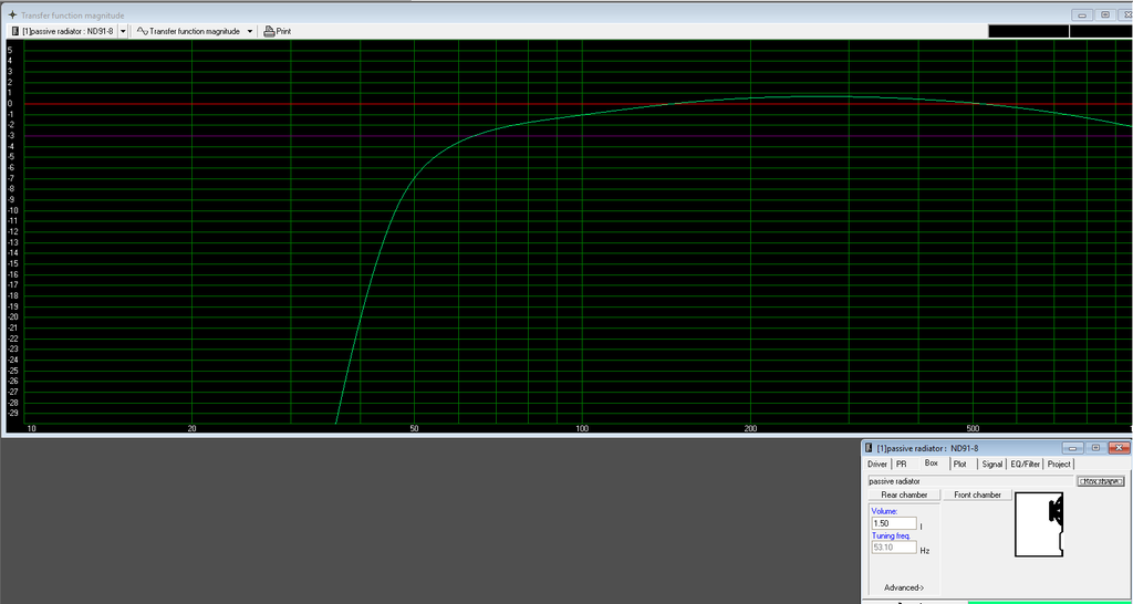
The simulation project and driver files are here:
Step 4: Input Section
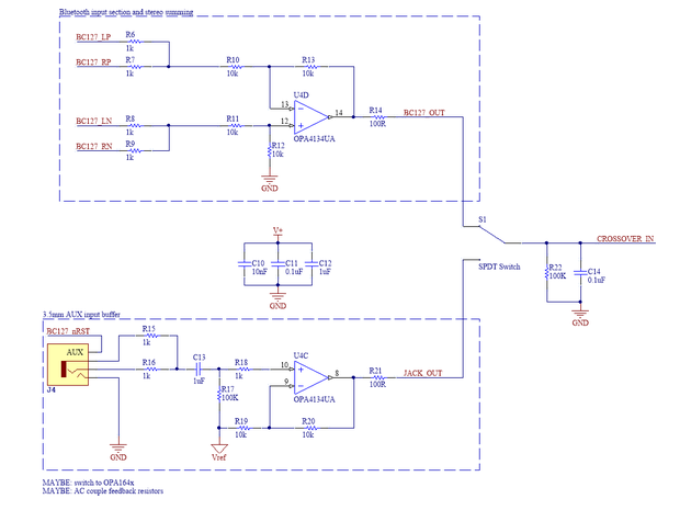
The input section serves several purposes. Since the speaker needs only one channel of audio, this sums the left and right channels using resistors. It also allows for switching between the jack or the Bluetooth module.
The jack buffer AC couples the input signal using film capacitor C13 — a good way to isolate the circuit from DC voltages from outside sources. This also biases the input signal to the reference voltage, VREF. Biasing refers to making an AC signal oscillate around a fixed DC signal — this is necessary for op amps to operate with only a positive power supply. The buffer is really a non-inverting op amp amplifier, so the gain can be adjusted using R19 and R20 if you want a louder signal.
The BC127 buffer converts the differential signal from the BC127 to a single ended signal that can be used by the op amp filters. It so happens that the inputs from the BC127 are already biased to 1.2V, meaning this stage will work even without bias. However, after building the board I realized that the BC127 could have been AC coupled for better performance as below:

This would be more effective at isolating the ground noise from the BC127 and also bias the output of this stage to the same voltage as the jack output.
A shortcoming of this circuit is the op amp choice — the OPAx134 family is only able to swing to within 1V of its rails — this means that this op amp will start distorting and clipping if the signal reaches below 1V or above 11V on a 12V power supply. If this circuit is to work at lower voltages (down to 7V) or if my first BC127 buffer implementation is used, the op amp starts clipping very quickly without much volume. Therefore, a rail-to-rail operational amplifier, more optimized for smaller voltage rails, should have been used.
Note that the 3.5mm jack symbol shows the 4th pin of a 4 pin JST PH connector used to connect the jack to the board (I had lots of them). These extra pins are conveniently used for sending non-essential signals off the board so that they can be accessed by devices not on the PCB. I do this for almost every PH connector I use here.
The output of the buffers connect to the input of the filter section in the next step.
Introduction: TPA3118 Amplifier and Speaker
 By FunkyPineappleFollow
More by the author:
Hi everyone!
After using a TPA3118 amplifier module for a while, I thought it would be fun to design my own PCB with the popular TPA311x series of amplifier chips as my first major electronics project. But why stop there? I ended up throwing on a Bluetooth module, a crossover, a bass booster and designing a portable speaker to use this amplifier in. The speaker box features the Dayton Audio ND91-8 full range, ND20FB-4 tweeter, and the Peerless 830878 Passive Radiator.
This project has been a huge opportunity to learn about circuitry, speaker design, and PCB layout. There was a very involved design process that is documented in a fair amount of technical detail in this Instructable. I hope sharing my experiences will help anyone who wants to embark on their own exciting journey of audio circuit design!
Demo video first!
Sound was recorded with a Zoom H4n right in front of the speaker. An unfortunate soldering accident left the poor thing Bluetooth-less for the time being. Many thanks to my friend Tim for the awesome video and photos!
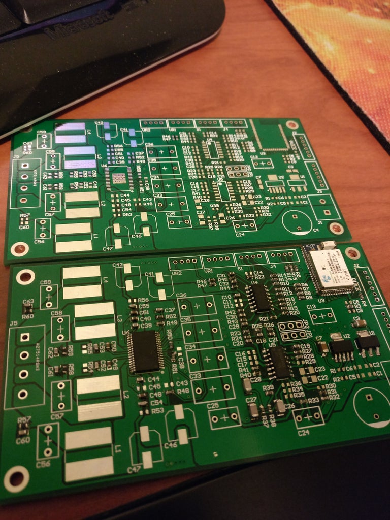
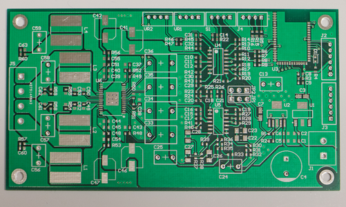
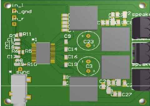
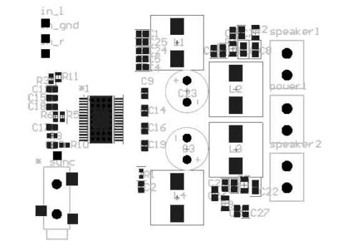
Step 7: PCB Layout
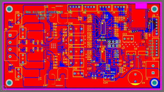
Once the schematic capture is complete, the time comes to put all of this on a PCB.
This is one of the first PCBs I have laid out. I spent a lot of time reading about PCBs before having enough confidence to try it. Here is some basic reading and some best practices.
Here are a few more I have picked up along the way:
— keep switching current loops as short as possible: the output LC filter of the Class-D amplifier should be very close to each other with short fat traces (I used polygons pours)
— leave some room between passive components and the IC («breakout») — gives more space for routing
— in fact, room between ALL components is good, if there is space — makes soldering/debugging/bodge wiring much easier
— unless you have a reflow oven, thermally relief polygon to component connection — otherwise that giant piece of copper acts like a heat sink and makes soldering painfully hard
— use common footprints and as few different footprints as possible — this makes for easy component swapping or changing passives
— don’t be afraid of vias, they’re very handy and don’t introduce THAT much disturbance in an audio circuit…however, they DO affect the circuit so don’t abuse them either…keep them at a minimum but there is no need to go out of your way to avoid them completely
— while this is often disputed, with a 2-layer board, I try to keep a ground pour on both sides for low impedance grounds
My mistakes:
— BC127 footprint (based off the datasheet) had pads that were MUCH too short and close together — caused many headaches soldering and eventually I broke all the BC127 modules I had
— no thermal relief on big components…wow they got hard to solder
— orientation of the inductor pads made them impossible to get a soldering iron to
— digital ground of BC127 was not separated from analog ground — this means ground noise bleeds into the analog circuit (Analog Devices application note about this)
Attached here is a GERBER and NC Drill package that I would send to a PCB manufacturer to get printed (I use OSH Park and PCBWay, both with reasonable prices). It is based on the schematic shown here, with the BC127 footprint modified to have longer pads and more inter-pad spacing. The PDF3D of my PCB is also attached.
Also attached is a BOM for the circuitry. Note that the electromechanical parts (potentiometers, switches, jacks) are not included.
Attachments
- TPA3118_BL_AMP_GERBERS.zipDownload
- Bluetooth_Amplifier_BOM.xlsxDownload
- Bluetooth_Amplifier_Board_3D.pdfDownload
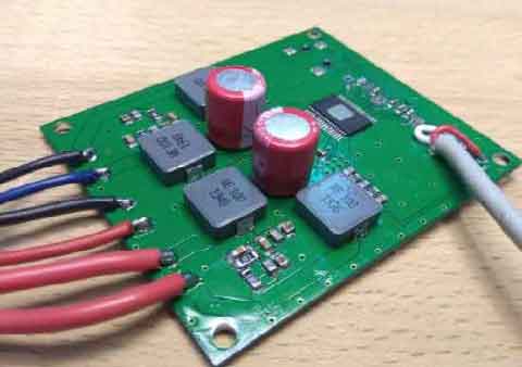
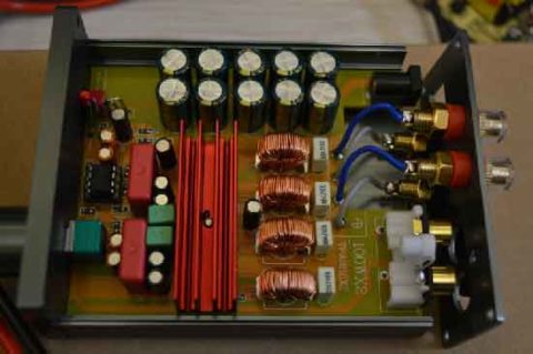
Схема TPA3116D2 — универсальный чип с прекрасным звуком H

Было бы правильнее заменить их фольгированными емкостями с большей линейностью, но только вот их расположение очень сложно изменить. Два электролитических конденсатора с низким импедансом 1000 мкФ/35v включены для развязки линии питания. Чип TPA3116D2 охлаждается радиатором, который, кажется, приклеен к корпусу микросхемы, что затрудняет самостоятельные эксперименты.
Тем не менее, перед первоначальным тестом было решено заменить конденсаторы выходного фильтра фольгированными конденсаторами 1 мкФ, чтобы немного снизить частоту среза. Конденсаторы развязки линии питания были увеличены двумя конденсаторами 2200 мкФ/35v, подключенными параллельно и расположенными на противоположной стороне печатной платы. В целом это составляет хорошие 6000 мкФ для развязки.
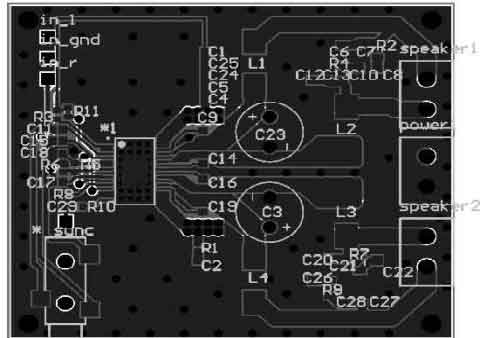
Самодельный аудио усилитель класса D на TPA3116D2
Наконец, была решена небольшая проблема, которая была замечена во время первоначального тестирования: заметное «шипение» в динамиках, если потенциометр громкости был помещен в среднее положение, например, если вход усилителя составлял сопротивление более 10 кОм. Известно, что усилитель с питанием от цепи с высоким импедансом может генерировать шипение. Потенциометр объема был измерен как 50 кОм.
50 кОм — это довольно высокий импеданс, учитывая, что в современных предварительных усилителях обычно используются OP-AMP, которые могут работать с низким сопротивлением на выходе — часто 600 Ом. Таким образом, необходимости в использовании потенциометра на 50 кОм не было.
Схема усилителя на микросхеме TPA3116D2
Но потенциометр имел функцию выключателя питания, и его было бы очень сложно заменить без риска повреждения дорожек печатной платы. Поэтому между входом усилителя и землей, ниже потенциометра, были установлены два резистора 4,7 кОм, так что на входе усилителя оставалось ниже 4,7 кОм. Это решило проблему шипения, но несколько изменило поведение потенциометра. Однако предусилитель, питающий плату TPA3116D2, имел другой регулятор громкости.
Микросхема TPA3116D2 также поставляется в виде небольшого модуля, в котором только основные компоненты устанавливаются вокруг кристалла с использованием технологии SMD. Тогда, любители самостоятельной сборки, могут выбрать наиболее важные элементы и реализовать оптимизированное охлаждение.
 |
 |
 |
 |
Основные характеристики:
- Напряжение питания 4,5-26v, 2×30 Вт на 8 Ом, 0,1% THD, ток покоя 30 мА.
- Смещение постоянного тока, измеренное на выходах: 1 мВ/5 мВ (питание 24v).
Такие усилители мощности подходят для использования с сабвуферными динамиками и имеют очень хорошие характеристики. Усилитель мощности TPA3116D2 также имеет широкий диапазон напряжений от 5v до 24v и рекомендован для схемы сабвуферного УМ, использующей эту микросхему TPA.
Загрузки:
Схема и печатные платы: Schematic_PCB
Печатная плата TPA3116D2: 3D модель 3D_Step_Model
Предыдущая запись Схема усилителя на микросхеме TDA7294 мощностью 100 Вт
Следующая запись Схема мостового включения 4 LM3886
Step 5: Filter Section
Ah, this one is a mess 😛
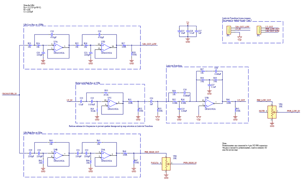
While this circuit looks complicated, it really is just a few small blocks put together.
I selected a frequency of 5KHz for the cutoff to the tweeter — plenty of room so that the tweeter isn’t playing anywhere close to its resonant frequency of 2KHz. The crossover is a classic 4th order Linkwitz-Riley crossover. These cascaded 2nd order filters have a steep 24dB/octave slope. While I can write all the theory here I thought it would be better coming from the original creators or Rod Elliot of ESP. In short, these are high pass and low pass filters with a steep slope, made using op amps.
Following the low pass filter for the woofer is the interesting part of this circuit. A 2nd order high pass filter at 55Hz rolls off the really low frequencies. There’s really not much audio below 50Hz so we might as well protect the speaker and the next op amp from trying to play too low.
Since a high pass filter cuts off all low frequencies, including DC, which is effectively 0Hz, the output signal of that stage actually ends up biased at 0V. Well, there goes all the hard work biasing this signal. Unfortunately this means we have to AC couple and bias it again to 4.5V, which thankfully isn’t all that hard.
The next stage is the Linkwitz Transform, a unique circuit with with some complex math that acts as a bass booster. Usually used to correct low end roll-off in a non-ported speaker box, I am…misusing…it to simply get more bass out of this circuit.
Not knowing whether or not the bass cut and boost will actually help the sound of a particular speaker box, I left in 2 jumpers that bypass this section of the circuit.
The two channels of audio — now separated low and high frequencies, are connected to the TPA3118 via potentiometers as individual volume knobs for the tweeter and woofer.
Step 3: Power Supply and BC127
Note: full schematic is attached as PDF.
Power Supply
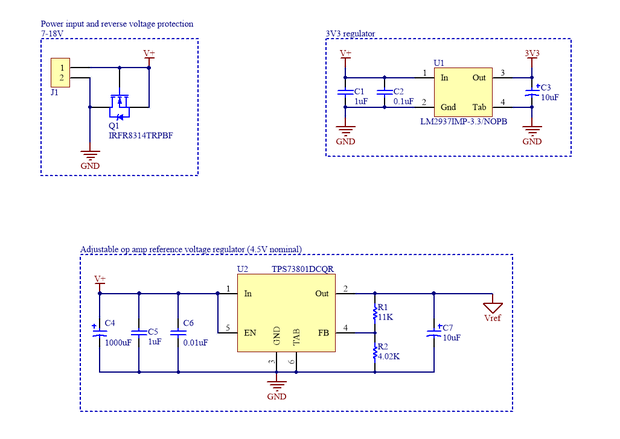
J1 is the power input jack. I am using a terminal block so that I can swap power supply modules, but really any jack will do as long as it satisfies the voltage requirements. That being said, 7V would result in a very quiet amp because the operational amplifiers will clip very quickly, and 18V will cause too much heat dissipation from the linear regulators (U1 and U2). The sweet spot is around 12V. The circuit will theoretically work up to about 24V as the TPA3118 is rated to that voltage. However, make sure the capacitors are rated up to that voltage.
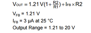
Since a linear regulator is effectively a buffered voltage source, it is perfect to use as a virtual ground/reference point for op amps. Ideally, this reference point should be about halfway between the power rail and ground. Regulator U2 is has an adjustable output, set by R1 and R2. The equation for calculating output voltage is:
(From the TI datasheet)
MOSFET Q1 is used as reverse voltage protection…just in case clumsy me inverts the power lines 😛
A 1000uF bulk capacitor serves as a local voltage supply for the board, so that the circuit can draw a large current from a source without the power supply voltage dipping. Read this for more information about bulk capacitors.
BC127
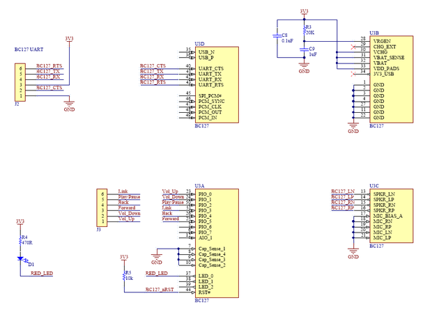
The BC127 implementation is very simple, since we are only using it as an audio module. The UART interface is broken out to a connector to allow for firmware updates to the BC127. A commonly available UART-to-USB adapter is needed for this.
The IO pins for audio control is broken out via J3. A microcontroller or physical buttons can be connected to these.
R3 pulls up the VREGEN (regulator enable) pin of the BC127, which needs to be at a logic high for the module to boot. C9 is used to slow down the rising edge of that signal so that the power supply has time to stabilize before the module is booted (totally overkill).
The speaker out connections continue to the input section of the circuit on the next step.
Похожие записи:
 Интересные поделки из бумаги сделанные своими руками: идеи, фото, пошаговый мастер-класс
 Восстановление акрилового покрытия ванны
 Рецепт сала в луковой шелухе: как добиться копченого вкуса без копчения
 Скумбрия в горчице на костре
 Брудер своими руками пошагово: размеры и советы
 Чем отличается серый пеноплекс от оранжевого